|
Artificial Intelligence for Wafer Production Monitoring
Abstract The chips contained in every electronic device are manufactured over circular silicon wafers. The growing demand of semiconductors in nearly all the industrial sectors has made human quality inspection of wafers infeasible. Thus, electronics and semiconductors manufacturers require advanced Artificial Intelligence techniques to automatically monitor their entire production. Here we present the research projects established in a collaboration between Politecnico di Milano and STMicroelectronics, in which we design deep learning models to recognize and interpret defect patterns in silicon wafers during manufacturing.
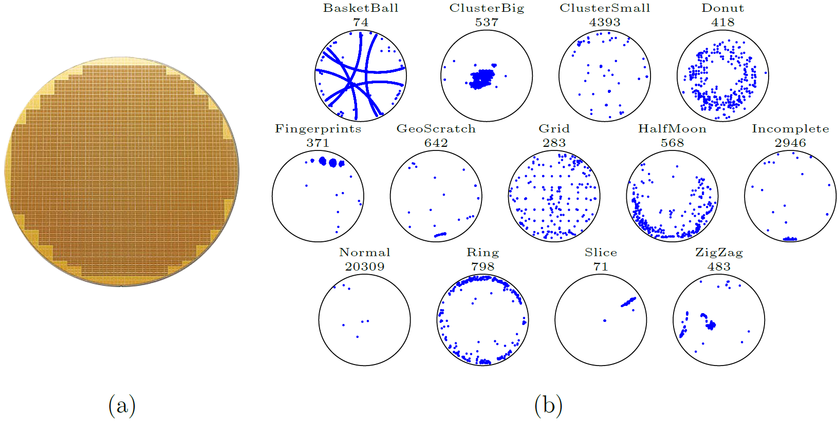
Fig.1: (a) a Silicon Wafer; (b) examples of Wafer Defect Maps (WDMs) from the classes included in the ST dataset, and total number of samples in each class. Wafer Defect Maps Classification The primary research goal we addressed was the automatic detection of problems and failures in the production process. Quality inspection machines can exclusively identify localized defects, returning a list of defective locations in each wafer, namely a Wafer Defect Map (WDM). Production issues such as a robot accidentally scratching the wafer surface, can be detected by analyzing patterns over the WDM. Not surprisingly, the classification of defect patterns has been widely investigated in the literature but in rather simplistic settings where i) all the classes of defect patterns are assumed to be known and represented in the training set and ii) WDMs are transformed into low-resolution images.
The major outcomes of this research collaboration are:
|
|
References [Frittoli et al. 2022] Deep Open-Set Recognition for Silicon Wafer Production Monitoring [Moioli et al. 2021] Wafer manufacturing system, device and method [Morbidelli et al. 2021] Augmented Grad-CAM: heat-maps super resolution through augmentation [di Bella et al. 2022] Wafer defect map classification using sparse convolutional networks [Frittoli et al. 2022b] Artificial Intelligence for Silicon Wafer Production Monitoring |
